
參賽序號:2-12
海報主題
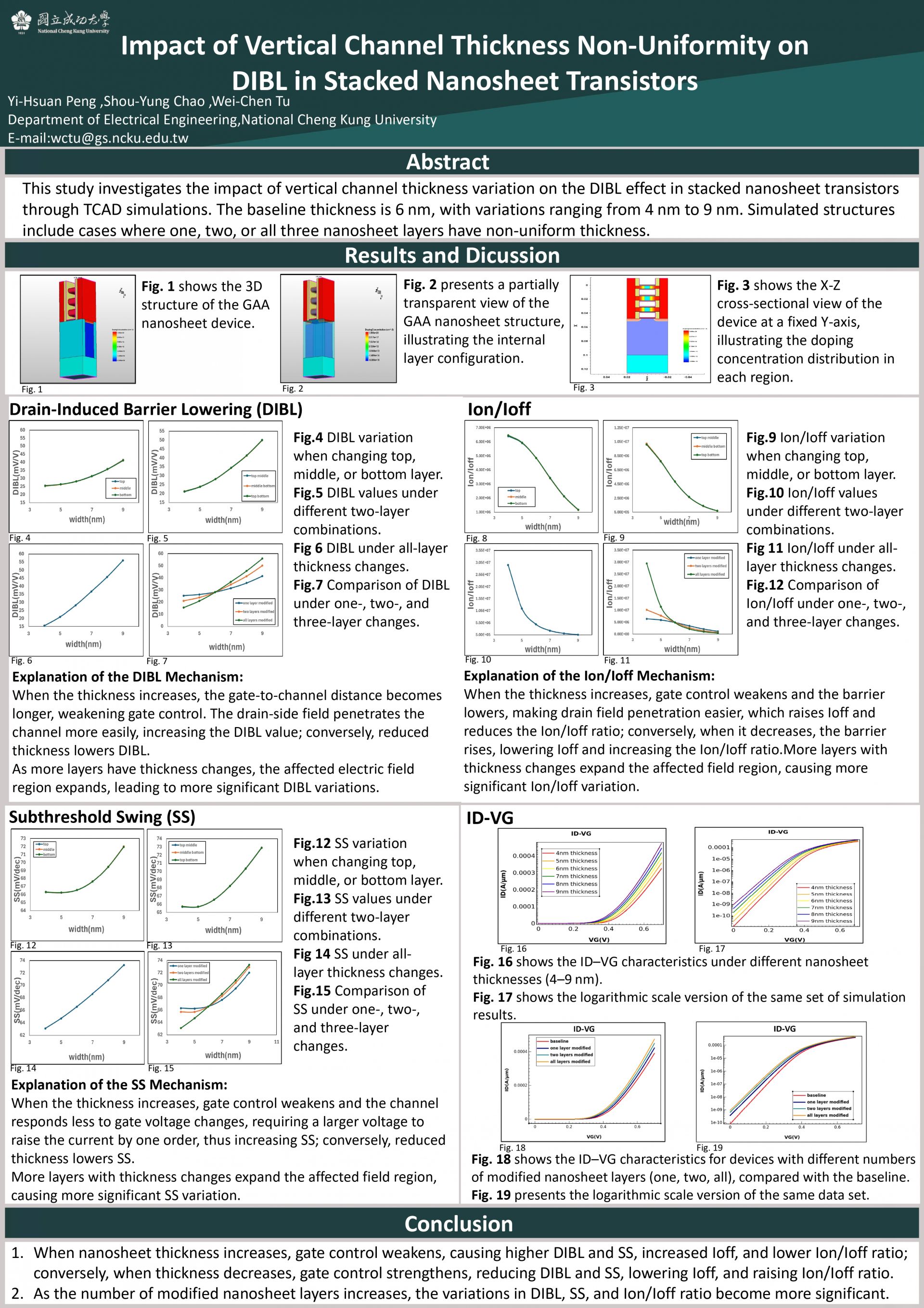
垂直nanosheet中縱向通道厚度非均勻性對DIBL效應之分析 Impact of Vertical Channel Thickness Non-Uniformity on DIBL in Stacked Nanosheet Transistors
系級
電機工程學系
指導老師及參賽學生
指導老師:涂維珍
參賽學生:彭羿璇
構想說明
This study explores the influence of vertical channel thickness non-uniformity on short-channel effects, with a focus on Drain-Induced Barrier Lowering (DIBL), in stacked nanosheet gate-all-around (GAA) transistors. Using TCAD simulations, a three-layer nanosheet device was designed with a baseline channel thickness of 6 nm, and various configurations were introduced by adjusting the thickness from 4 nm to 9 nm. Simulated cases include scenarios where one, two, or all three nanosheet layers experience thickness variation. The results show that increased channel thickness weakens gate electrostatic control, allowing the drain-side electric field to penetrate more easily and lower the channel barrier, leading to increased DIBL, degraded subthreshold swing (SS), higher off-state current (Ioff), and a lower Ion/Ioff ratio. Furthermore, as more layers are modified, the degradation becomes more pronounced. In contrast, reducing the channel thickness improves electrostatic control and leads to better electrical characteristics in terms of DIBL, SS, Ioff, and Ion/Ioff ratio. Keywords: Drain-Induced Barrier Lowering(DIBL), Channel Thickness Non-Uniformity, Gate-All-Around (GAA) Nanosheet Transistors
-
分享:


 114年活動,現正報名中!